Home » Blog » Upload the Bootloader of Pixhawk
Upload the Bootloader of Pixhawk
— Last modified: xiaoke [das.xiaoke@gmail.com] 2015/12/08 08:53
There has already been fairly detailed descriptions of updating and uploading Pixhawk bootloaders on its official website.
Recently I had an incident and had to replace the ARM processor on the Pixhawk board. After the exhausting work of desoldering and soldering the 144-pin QFP STM32F427 ARM chip, I found this piece of hardware actually lost every bit of the software. And I'll have to start from the bootloader in order to reprogram the chip.
First, what is a bootloader?
According to various definitions found online, a bootloader for an embedded system is a section of code responsible for self-testing and preparing the environment for the running of the processor. The STM32 device comes with a built-in bootloader in the internal boot ROM memory space, which is programmed by ST during the production phase. The main purpose of this bootloader is to enable the download of the user's program into the flash memory through USART, USB and other serial connections, rather than the much more complicated JTAG device. Detailed descriptions on this built-in bootloader can be found in the ST Application Note AN2606 http://www.st.com/st-web-ui/static/active/en/resource/technical/document/application_note/CD00167594.pdf
There are two pins on the ARM chip, BOOT0 and BOOT1, configuring the boot mode of the processor. When BOOT0 is high, the processor boots from the built-in bootloader and it is then possible for the user to download the application program into the flash memory via serial connections. If BOOT0 is low, the processor starts running at 0x08000000, i.e. the beginning of the flash memory space and the built-in bootloader is not executed.
'The PX4 Bootloader'
The 'bootloader of pixhawk' is not the built-in bootloader as described in the above, but rather a program developed by the PX4 team. This 'bootloader' resides in the user's program space, i.e. the flash memory space starting from 0x08000000. The main purpose of this bootloader is to enable the user to flash the PX4 firmware into the chip, e.g. via QGROUNDCONTROL or the download script provided by the PX4 source code.
For detailed description of this bootloader, please read the source code on github at https://github.com/PX4/Bootloader.
NOTE that the design of the Pixhawk hardware connects the BOOT0 pin to GND via a 10k resistor. So by default, the built-in bootloader of ST is not executed, which means that it is not possible to flash the program via USB, or USART connections by default. However, by simply short-circuiting the BOOT0 and VCC test pads when powering up the board, the built-in ST bootloader can be activated. This is the simplest approach to programming the PX4 bootloader, but we'll discuss here a more complicated approach via the JTAG cable.
Flash the 'PX4 Bootloader' via the JTAG cable
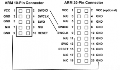
The pixhawk board has a 10-pin mini JTAG port, whose connector is not soldered. The connector is a 2×5 1.27mm surface mount header. See http://portal.fciconnect.com/Comergent//fci/drawing/20021321.pdf for details. Currently I have a ST-LINK V2 programming device which has a 20-pin JTAG port for STM32 devices. It seems that only two pins are actually used, SWDIO, SWDCLK, which constitute the Serial Wire Debug (SWD) specifications. We can simply build a cable connecting these two pins and the GND of the two types of port, but there are adapting boards available online, e.g. the one at https://www.olimex.com/Products/ARM/JTAG/ARM-JTAG-20-10/. Note that SWD is another debug port specification, which is different from JTAG and supported by ARM Cortex processors. See http://www.arm.com/products/system-ip/debug-trace/coresight-soc-components/serial-wire-debug.php.
So the overall connection is rather simple, as shown in the following figure.
Then we come to the software part. Basically what we need is (1) Software for ST-LINK V2 programmer, (2) Source code for the bootloader. The Pixhawk site has detailed descriptions on both, which can be found at https://pixhawk.org/dev/px4_bootloader. In Linux command line, the command for flashing the bootloader is
st-flash write px4fmuv2_bl.bin 0x08000000
STM32F4XX Memory Space Allocation
Furthermore, a very brief descriptions of the memory space allocation of the STM32F4xx chip is as follows, in order to explain the number 0x08000000 in the code above. The STM32F407x chip has a 32-bit multi-layer bus structure (called AHB bus) connecting various lower-level buses. This structure is thus capable of addressing a 32-bit space, which is equivalent to 4G Bytes. This space is further allocated according to a memory map, which can be found in the datasheet of the device, e.g. http://www.st.com/web/en/resource/technical/document/datasheet/DM00037051.pdf
The flash memory and the on-chip RAM are listed as follows
| Type | Size | Address |
|---|---|---|
| System Memory | 30K | Starting from 0x0000 0000 |
| Flash Memory | 1M | 0x0800 0000 - 0x080F FFFF |
| CCM data RAM | 64K | 0x1000 0000 - 0x1000 FFFF |
| SRAM1 | 112K | 0x2000 0000 - 0x2001 BFFF |
| SRAM2 | 16K | 0x2001 C000 - 0x2001 FFFF |
Basically, this means that the code is stored from 0x08000000 onwards. The SRAMs starting from 0x20000000 and 0x2001C000 are general purpose RAMs while the CCM RAM space starting from 0x10000000 can only be accessed by the CPU.
After flashing the bootloader, QGROUNDCONTROL is capable of recognising the Pixhawk board and flashing the firmware .